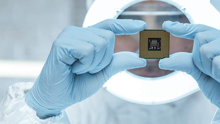
Scientists have made nanowires for chips the size of a molecule
Researchers from NUST MISIS, together with colleagues from the USA and China, have developed a technique for creating ultrathin semiconductor crystals that provide high current density and are resistant to external influences. They are based on compounds of nickel, tantalum and selenium.

The thickness of such nanowires is 100-400 nm, and the length is up to several millimeters. Such dimensions will make it possible to manufacture ultra-miniature electronic devices based on them. This includes sensors the size of a molecule, which, in the composition of various materials, can give them new properties.
For example, in engineering, nanoelectronic chips will make it possible to create "smart" surfaces that will "report" the occurrence of microcracks, and in medicine, miniature devices that will help carry out complex diagnostics in hard-to-reach areas of the body.
"Silicon used to be the main material for electronics. However, now devices based on it have reached the technological limit. Their further decrease leads to a deterioration in performance. Therefore, researchers are looking for materials that exhibit their electronic properties at the nanoscale," said Pavel Sorokin, head of the NUST MISIS Laboratory of Digital Materials Science.
According to him, the new material belongs to one-dimensional structures, the use of which was previously limited due to the complexity of their synthesis and the fragility of crystals. At the same time, the obtained samples showed high stability and resistance to moisture, ultraviolet and other factors.
Переведено сервисом «Яндекс Переводчик»
