Nano same: gold nanodisks will allow you to create robots the size of a speck of dust
- Статьи
- Science and technology
- Nano same: gold nanodisks will allow you to create robots the size of a speck of dust

Russian scientists have developed an innovative method for analyzing nanostructures, which makes it possible to increase the capabilities of modern atomic force microscopes and study substances on a scale of units of nanometers. The introduction of a new technology opens up opportunities for designing new useful materials with specified properties at the atomic level. Such methods are in demand, in particular, when creating the electronics of the future. For example, microscopic devices such as "dust motes" sensors and molecular robotics.
How the new nanostructure analysis method works
Scientists from the A.V. Rzhanov Institute of Semiconductor Physics of the Siberian Branch of the Russian Academy of Sciences have developed a new ultra-precise spectral optical non-destructive method for analyzing materials. It significantly expands the capabilities of existing atomic force microscopes, allowing materials to be studied on a scale of units of nanometers and to study not only their structural dimensions, but also their chemical structure.
In particular, such precision is in demand when creating miniature devices and equipment. For example, molecular robotics for high-precision drug delivery in the human body, "dust mote" sensors for monitoring objects and covert surveillance, or insect drones for spaces and surfaces inaccessible to humans.
— One of the methods of studying nanostructures is Raman spectroscopy. It consists in analyzing the spectrum of laser radiation reflected from the structure under study. This radiation, like fingerprints, contains all the information — from the composition of the substance and impurities to various defects, deformations and stresses," Alexander Milekhin, one of the developers, Deputy Director for Scientific Work at the Institute of Physics and Technology of the Siberian Branch of the Russian Academy of Sciences, told Izvestia.
However, he explained, there are fundamental limitations to optical observation methods. For example, the so-called diffraction barrier, which prevents two objects from being distinguished if the distance between them is less than half the wavelength of light. For the visible range, this limit is about 200-300 nm. The second problem is to reduce the strength of the scattered signal at the nanometer level. However, thanks to the combined use of spectroscopy and atomic force microscopy, the researchers were able to overcome these limitations.
The principle of operation of atomic force microscopes is that its oscillating probe (a needle with a tip of 50 nanometers), when approaching the material, encounters the force of interaction with the surface, explained Alexander Milekhin. It changes the frequency and phase of the probe oscillation. By interpreting these data, it is possible to reproduce in detail the relief of the material and its properties.
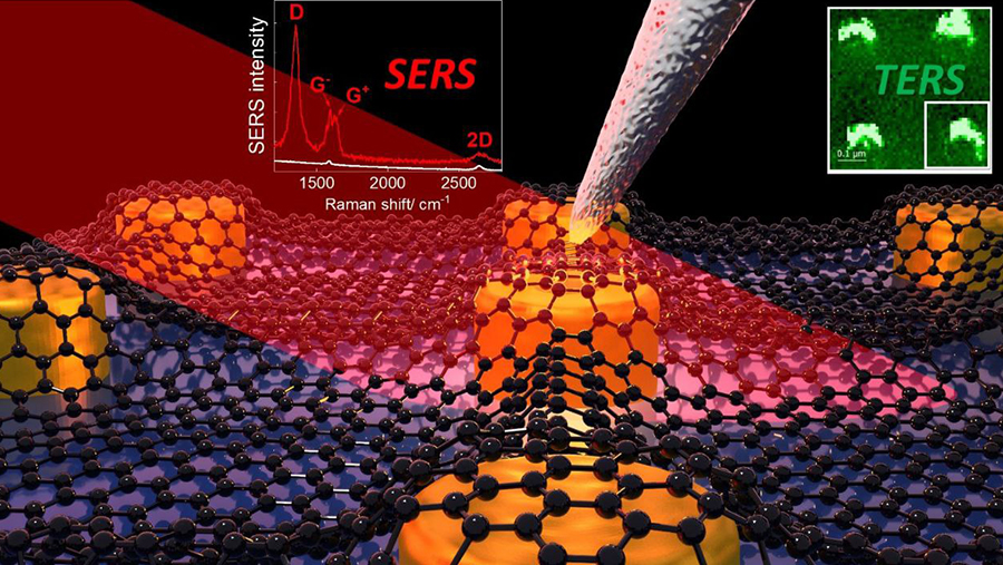
— In order to determine the spectral characteristics of the material (for example, the chemical composition at each point), we apply silver, gold or platinum to the probe in such a way that a single cluster of metal about 100 nm in size forms on its tip. A strong electric field is formed under it in a small area. On the other hand, we used arrays of gold nanodiscs as a substrate for the structures under study," the scientist described the essence of the development.
According to him, when the metallized probe approaches the gold nanodiscs, a so—called hotspot is formed between them - a plasmon, an area of a concentrated electromagnetic field of high intensity.
If the energy of such a "slit" plasmon corresponds to the excitation energy in the material, the scattering intensity increases sharply, which allows obtaining more detailed information. The task of the researchers was to create the necessary conditions. As a result, they received a signal amplified by 100,000 times, with a spatial resolution of 2 nm.
What areas require high-precision methods for studying materials?
According to Alexander Milekhin, the new method was used to study atomically thin structures of semiconductor materials that are of interest to modern microelectronics and photonics. For example, when analyzing graphene, scientists found a stretching of its crystal lattice by only 1.5%. This is small, but it is critically important for the electronic properties of the material.
Such studies help to better understand how two-dimensional materials work in real conditions and help improve their quality. In the future, this will help create more accurate and sensitive sensors, flexible electronics, and even elements for future nanorobots.
— We are currently working with scientists from the A.F. Ioffe Institute of Physics and Technology to create miniature lasers (and other nanophotonics elements) based on transition metal dichalcogenides. Our task is to monitor and develop recommendations for improving their optical properties," the scientist gave an example.
In his opinion, in the future, the new method may be in demand in materials science, chemistry, geology, pharmacology and other fields where high-precision research of materials is required. Other interesting areas include determining the quality of food products, petroleum products, explosives, and pesticides.
— This approach is based on an ingenious combination of two technologies: surface-enhanced (SERS) and probe-enhanced (TERS) Raman spectroscopy. The secret of the technology lies in gold nanodiscs and an ultra-thin metal probe. Gold nanoparticles work as tiny antennas, amplifying the signal by 50 times, and a needle—sharp probe adds even more amplification — up to 100 times," Sergei Polyutov, director of the International Scientific Center for Spectroscopy and Quantum Physics at Siberian Federal University, explained to Izvestia.
According to him, the key mechanism of the method is based on plasmon resonance, collective vibrations of electrons in a metal that amplify the signal.
However, the expert noted that, like any advanced technology, gm-TERS still has its limitations. For example, the preparation of samples for these experiments requires exceptional accuracy: graphene must evenly cover nanodiscs with a diameter of 108 nm (tolerance is only ± 5 nm), and the slightest "folds" or contamination distort the data. At the same time, silver probes, although they provide fantastic signal amplification (comparable to the ability to hear a human whisper from 100 meters away), cost thousands of dollars and quickly fail.
Despite these difficulties, the potential of the technology is revolutionary, said Sergey Polyutov. In the near future, it may, for example, become the standard for graphene quality control in industry. The new method can also accelerate the creation of hybrid materials (for example, combinations of graphene with quantum dots) and will allow the development of ultra-sensitive biosensors for early diagnosis of diseases, he added.
— The advantages of the method include flexibility with respect to the exciting wavelength of radiation. The authors show that by selecting the diameter of the nanodiscs, it is possible to obtain amplification at different wavelengths. This makes it possible to use the proposed method for spectrometers with various lasers, as well as to select the resonant excitation frequency that coincides with the maximum absorption of materials," said Ilya Zavidovsky, senior researcher at the Center for Photonics and Two—Dimensional Materials at the Moscow Institute of Physics and Technology.
At the same time, the list of restrictions should include additional technological steps necessary for sample preparation, the expert believes. For example, the deposition of gold film, the implementation of nanolithography for etching discs, the transfer of layered material to an array of discs.
— The modern world is a world of nanotechnology and quantum physics. Almost all modern devices, devices and machines have unique characteristics due to the fact that they are designed at the smallest level (down to individual atoms and molecules). For example, a trillion transistors can work in one flash drive," Andrei Naumov, head of the Troitsk branch of the Lebedev Institute of Physics, Doctor of Physico—Mathematical Sciences, told Izvestia.
Thanks to the development, he explained, scientists can learn how individual atoms and molecules are folded into more complex structures with specified properties. It is these materials that will change the life of mankind, he concluded.
Переведено сервисом «Яндекс Переводчик»
