Light in optical fiber: new device will reveal defects on high-speed Internet lines
- Статьи
- Science and technology
- Light in optical fiber: new device will reveal defects on high-speed Internet lines
Russian scientists have proposed a new signal processing method for diagnostics of fiber-optic lines and photonic chips. The method effectively suppresses noise, but it does not distort defect data, which makes it possible to obtain a "clean picture" of damage. The solution can be useful in telecommunications, the oil and gas industry, and in the verification of integrated optical circuits. In the future, scientists plan to adapt the algorithm for different devices. However, in order to effectively promote development, you need your own hardware or software licensing, experts noted.
How to check fiber-optic communication lines
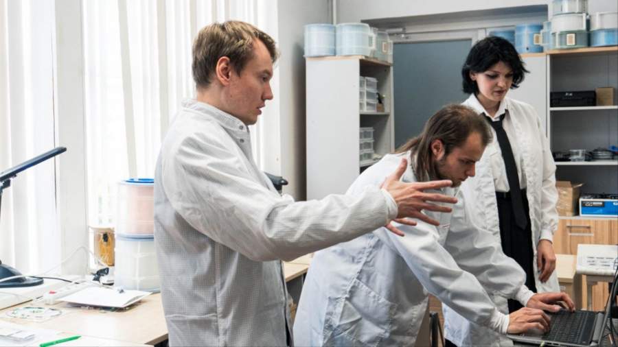
A new approach to fiber testing was proposed by scientists from the Institute of Continuum Mechanics of the Ural Branch of the Russian Academy of Sciences and Perm National Research Polytechnic University. The development will allow testing lines hundreds of kilometers long with high accuracy. Its other purpose is to test photonic chips, devices that use light particles to transmit a signal.
Optical fiber is glass filaments with a diameter of 125 microns, which is thinner than a human hair. Terabytes of data per second can be transmitted using light pulses. This ensures high-speed Internet, connectivity between continents, and the operation of data centers.
In Russia, the length of such networks is about 1.5 million km. Optical technologies are used in many strategically important areas. For example, in the oil and gas industry, distributed networks of photonic sensors connected by fiber-optic lines monitor the condition of wells and pipelines for tens of kilometers. Similar technologies underlie the "Internet of things", are used in construction to monitor deformations, as well as in security systems and medical equipment.
"But even the most advanced photonic structures have weaknesses. For example, in the manufacture of a fiber or a tiny optical chip, imperceptible defects may appear: an uneven wall, a speck at the junction, or internal stress. In a fiber-optic part (for example, in a splitter) Over time, a microcrack may occur from vibrations or temperature fluctuations," Anton Krivosheev, one of the developers, a junior researcher at IMSS Ural Branch of the Russian Academy of Sciences and an employee of the PNRPU Department of General Physics, told Izvestia.
From the outside, everything looks intact, but inside, unnecessary light reflections and uncontrolled signal loss begin. As a result, for example, the pressure sensor on an oil pipeline begins to give erroneous readings, and the gyroscope in the navigation system accumulates an error.
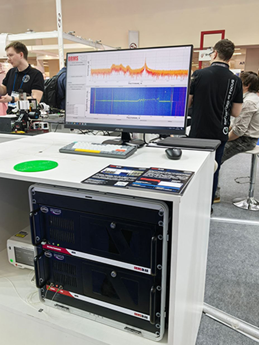
According to Krivosheev, specialists use a special device to find the damage. It sends a laser beam into the fiber and determines where they are by reflecting light from microcracks, joints and other defects with an accuracy of micrometers.
— The problem is that very little light comes back. It is so small that the data is comparable to the device's own interference, which is called noise. It's something like a ripple or crackle on the screen. It is almost impossible to distinguish real defects from noise without special processing," said Artyom Turov, co—author of the study, a junior researcher at IMSS and an assistant at the Department of General Physics at PNRPU.
At the same time, he added, well-known methods remove noise roughly.: they smooth out the signal, but along with the interference, they lose the feedback from real damage. As a result, the error can reach 53% for some of them. That is, the defect will look two times less dangerous, which is why specialists may skip the marriage. For optical chips, such errors are unacceptable, since the devices will work with errors or fail altogether.

How a smart algorithm will clear a light signal
As a result, a new approach to signal purification has been proposed. Instead of rough averaging, which "smears" the signal, the researchers proposed a smart algorithm.
— For each section of the signal, it determines what is in front of it — chaotic noise or a sharp jump from a defect. If there are a lot of chaotic fluctuations around, it means it's noise. The algorithm smooths it out, but does not affect the overall signal strength. If a rare sharp jump is visible, this is real damage, the algorithm leaves such a section untouched," explained Anton Krivosheev.
According to him, the new method has been tested on real equipment. Tests have shown that it provides zero peak distortion and signal level offset. This means that the specialist sees a clean picture during the check.
Based on the development, scientists have created a prototype device for diagnosing optical chips. Its cost is one third lower than its global counterparts. In addition, the proposed algorithm can be implemented into the software of commercial reflectometers, devices for measuring communication line parameters. This eliminates the need to purchase new equipment.
— Optics is now an integral part of the telecommunications infrastructure. Therefore, any technology that relies on cloud services or some kind of server infrastructure to combine devices into a single system will certainly benefit from the development of optical systems," said Ivan Dyakonov, a researcher at the Center for Quantum Technologies at the Faculty of Physics at Moscow State University.
In his opinion, it is important that the proposed method can be used to detect problem areas in fiber communication lines and build networks with high fault tolerance. For example, if you find a defect, you can use it to switch to a backup channel. It is also important that the new approach makes it possible to test miniature integrated optical systems.
— Optical fiber has already replaced copper in primary networks, with its help they transmit much more data and thousands of times further — without repetition and with much better quality. So the future of the Internet and communications belongs to photonic technologies," said Dmitry Chernikov, Head of the Basic Department of Infocommunications at Siberian Federal University.
In his opinion, the development of scientists helps to eliminate one of the main barriers of technology — signal attenuation due to inhomogeneities in the manufacture of fiber. Continuous production monitoring and testing will reduce losses and increase transmission distance. They will also simplify installation, since when welding fibers on lines under construction, you will not have to make unnecessary measurements.
It is worth noting, the expert added, that most manufacturers do not allow algorithms to be changed in their devices. Therefore, in order to apply the proposed methods, you need to produce your own hardware or licensed software.
"Photonic structures offer advantages in bandwidth, energy efficiency, and noise immunity compared to their electronic counterparts. The development of this infrastructure directly correlates with global digitalization trends and the need for high—speed data transmission," said Artem Kuznetsov, Head of the Department of Radiophotonics and Microwave Technologies at Kazan National Research Technical University — KAI.
According to him, photonic technologies are an important link in quantum communication and the Internet of Things. Also, in the context of a smart city and industrial robotics, they provide accurate monitoring of deformations, temperatures, and acoustic fields with high spatial resolution.
However, the expert emphasized that the method has limitations. For example, attenuation coefficients must be additionally checked. Therefore, auxiliary tools should be used for the final calibration of the algorithm.
Переведено сервисом «Яндекс Переводчик»
