Did you work hard on the alloys: Atomic 3D scanner will help create nature-like materials
- Статьи
- Science and technology
- Did you work hard on the alloys: Atomic 3D scanner will help create nature-like materials

Russian scientists have created a 3D research scanner, a device that allows to obtain a "map" of complex composites at the atomic level. The development will be in demand for the control of materials in which uniformity of structure is important. For example, special steels in the core of nuclear reactors or heat-resistant alloys for aircraft engines. The new device will also help to master nature-like technologies and reverse-engineer materials created naturally, experts believe.
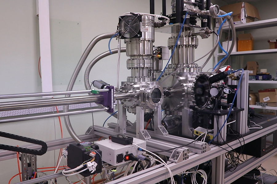
How does the device disassemble samples into individual atoms
Scientists at the National Research Nuclear University MEPhI have created a 3D scanner, a device that will allow them to "disassemble" a substance into atoms and build a three-dimensional map of the distribution of chemical elements in it. The development will allow specialists to obtain smart materials of a new generation. The Ministry of Education and Science of the Russian Federation told Izvestia about this.
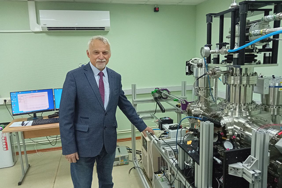
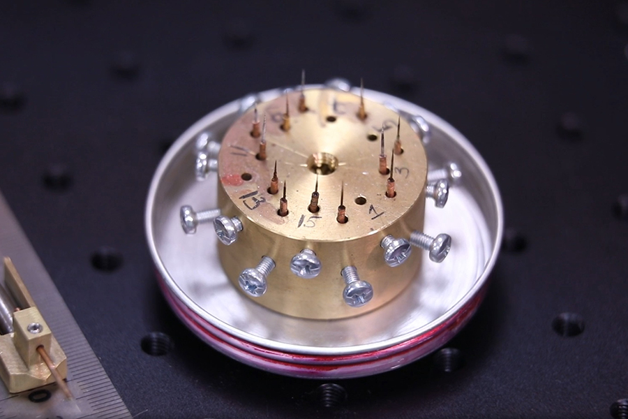
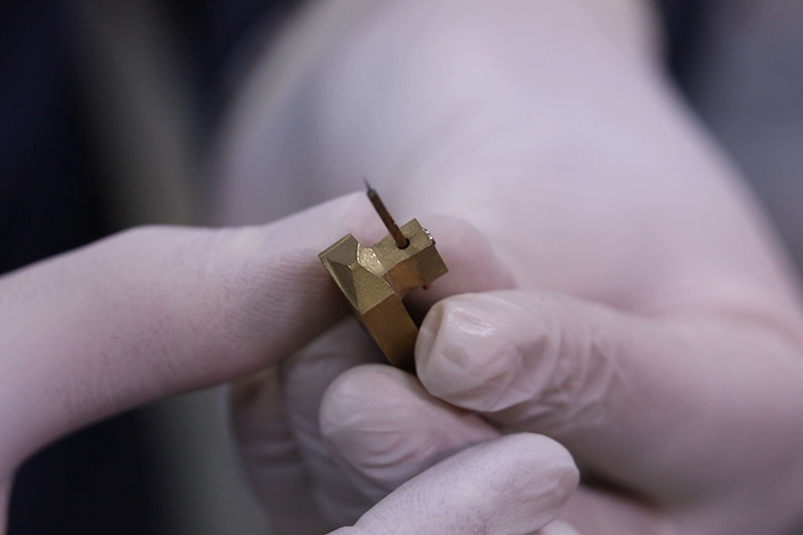
— The device works as follows: first, a sample is placed in it, then the substance is vaporized by laser pulses in nanoscopic portions. There are one or two atoms in each of them. At the same time, the chemical composition of the vaporized particles is determined by mass spectroscopy methods - by mass, which is calculated by the time of flight of these particles from the sample to the detector. At the same time, the samples are in a vacuum and cooled to cryogenic temperatures," Sergey Rogozhkin, Deputy Head of the Department of Physics of Extreme States of Matter at the National Research Nuclear University MEPhI, told Izvestia.
The data obtained is processed on a computer, as a result of which a three-dimensional map of the arrangement of atoms in the sample is formed. Such a model can include hundreds of millions of atoms. According to the scientist, such studies are especially important for studying complex composites and alloys. These materials contain many components, and their final properties can be significantly affected even by quantitatively insignificant impurities forming nanoscale structures.
— Experts have long realized that the properties of materials are largely determined by their structure. Take, for example, diamond and graphite — both are made of carbon, but because of the different atomic order, they are completely different minerals. Structural features at a deep level can dramatically change their properties, especially at the nanoscale. The breakthrough value of the development is that it provides a tool for controlling properties on this scale," explained Sergey Rogozhkin.
How nanostructures shape the properties of materials
According to him, modern materials science works on a very small scale. For example, the typical sizes in modern microelectronics chips are units of nanometers. And one nanometer is a chain of 3-4 atoms. To create such "thin" materials, we need tools for their accurate diagnosis and control.
— During the operation of a nuclear reactor, harmful defects can occur in its body under the influence of radiation and high temperatures, which make the material brittle. To "cure" it, you must first make a diagnosis — that is, see such structures, and then prescribe therapy. Our device allows you to do this: by understanding the cause, find a way to eliminate it. For example, using annealing," added Sergey Rogozhkin.
The device also opens the way to the creation of materials of the future based on nature-like technologies. In particular, the study of solid biological tissues, such as cartilage and bones, makes it possible to understand the principles of the distribution of individual elements in them and reproduce them in artificial structures. For example, in medical implants or in new materials for homes, cars or spacecraft.

One of the advantages of the installation, the researcher noted, is the predominantly domestic component base. This makes it possible to produce serial samples many times cheaper than foreign analogues, and to refine devices in accordance with the requests of operating organizations.
In addition, the specialists have developed and patented their own software, which allows both to manage the research complex and independently process the data obtained.
How atomic tomography will accelerate the creation of smart materials
— The development of smart materials is directly related to the ability to study and control the formation of nanostructured regions in them. The three—dimensional "map" of the elements allows us to understand which features of the structure determine its strength, heat resistance, durability and other characteristics," Vadim Popkov, head of the Laboratory at the A.F. Ioffe Institute of Physics and Technology of the Russian Academy of Sciences, Associate Professor at St. Petersburg State Electrotechnical University LETI, explained to Izvestia.
The value of such developments is that they shorten the path to industrial technologies. The more accurately scientists understand the structural organization of a material, the faster they can create effective alloys, coatings and ceramics for specific tasks, he added.
— The availability of a domestic alternative is important from the point of view of sovereignty and security. The proposed complex refers to an advanced and complex method for determining the chemical composition of materials at the atomic level. The creation of such a device is an important step for Russian science," commented Alexey Salimon, Senior lecturer at the Skoltech Center for Digital Engineering.
In his opinion, the availability of such tools is in demand in a wide range of tasks. For example, the strength of aluminum alloys, which are used for airplanes, automobiles, and other equipment, depends not only on the metal itself, but also on microscopic additive particles (precipitates) that are evenly "scattered" inside it.
"Specifically, the development of MEPhI scientists will help the creators of nanostructured materials in developing the most advanced production technologies," says Vladimir Platonov, Head of the Department of Ecology and Life Safety, Associate Professor of Chemistry at Samara University named after S.P. Korolev.
According to him, such materials may also be in demand in medicine, the nuclear industry, construction, aviation, and the space industry. For example, special steels in the core of nuclear reactors or heat-resistant alloys for aircraft engines.
— It is worth noting that the first laboratory sample of the installation was created within the framework of the Unified Industry Thematic Plan Rosatom. The purpose of the development is accelerated testing of materials. It was based on the concept that its degradation under the influence of radiation exposure and other factors has a cumulative effect and depends on the dose of radiation," said the Director of Scientific and Technical Project Development at the private institution Science and Innovation (part of Rosatom). Ivan Safonov.
At the same time, the hypothesis was accepted that degradation begins with "small" changes. As a result, early nanoscopic changes can predict how the material will behave after many years of use, he added.
At the same time, the expert noted, one should keep in mind the "bottlenecks" of the technology. For example, you need to understand whether it is fair to draw conclusions about the state of the entire massive object based on the behavior of individual clusters.
Переведено сервисом «Яндекс Переводчик»
