- Статьи
- Science and technology
- Miscalculation: the inspection of microelectronics was assigned to a robot inspector with AI
Miscalculation: the inspection of microelectronics was assigned to a robot inspector with AI
Russia has developed a line of robotic complexes for detecting defects in the manufacture of microcircuits. The equipment allows you to identify defects at different stages of production and on various production lines. The minimum size of the defects can be 3 microns. At the same time, the verification speed reaches 1 sq. cm per second. The software of the complex is based on neural networks trained on more than 6 thousand images. Machine learning capabilities allow you to adapt the equipment to test new types of devices.
How robots detect microscopic defects
Quality control is a key process in the manufacture of microelectronics products. However, modern microchips are so tiny and complex that they require high-precision systems that detect defects at the micro level.
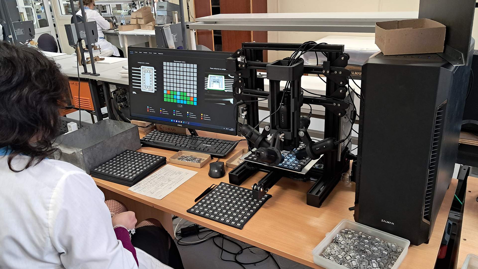
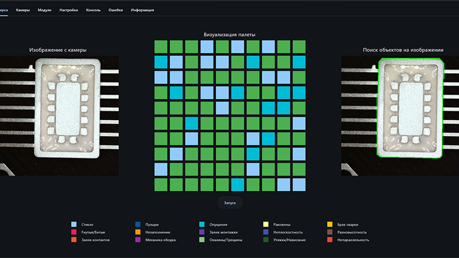
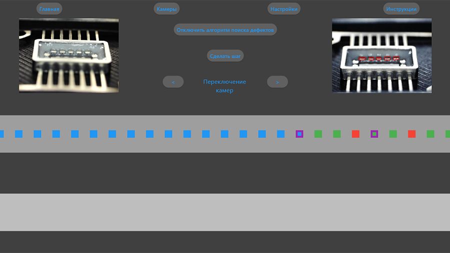
To solve this problem, Russian engineers have developed a family of smart inspection robots. These devices examine microchips at different stages of production. Using machine vision algorithms, each electronic component is analyzed for compliance with standards and the results are displayed on a monitor in real time. This allows not only to quickly identify defects, but also to eliminate the causes of defects in the future.
— When controlling the quality of electronics, the possibilities of human vision are limited when it comes to device sizes of several microns. The robotics complex is aimed at solving these problems. It is equipped with various cameras, electron microscopes and artificial intelligence capabilities to detect defects in the optical range, as well as a number of other sensors," one of the developers of the system, a senior engineer at Dayton Central Design Bureau (part of Element Group), told Izvestia Vyacheslav Malyshev.
At the same time, he added, the devices record the progress of the inspection, generate summary information on the detected flaws, calculate the yield of suitable products and analyze the growth or decline in the quality of manufactured products. This makes it possible to detect vulnerabilities in the technological process and eliminate them. Such measures help to increase the percentage of high-quality products and reduce the cost of production.

According to the expert, among the defects that robots detect may be defects such as cracks, scratches or chips that have formed due to violations of the production process, as well as unsealed fragments, distortions, inhomogeneities, broken tracks, dust and chemical residues. The dimensions of the tested products can range from 0.1 mm to 300 mm, and the maximum camera resolution is up to 3 microns. At the same time, the verification speed reaches 1 sq. cm per second.
— Robots perform all operations automatically. The complex is equipped with special software based on Russian patented developments. The software includes neural networks trained on more than 6,000 images," Vyacheslav Malyshev said.
He noted that, if necessary, machine learning algorithms make it possible to expand defect libraries. For example, when the product range is expanded or new regulatory requirements are introduced.
What types of devices are used to test microelectronics
At the moment, the specialist said, the family of robots includes three types of equipment. The first type of device scans chips stacked on a pallet, a substrate on which up to several hundred microelectronic components can be placed in special cells. At the same time, the manipulator moves sequentially, allowing the sensors to examine each product in detail. The second type of automatic inspectors is designed to monitor silicon wafers. They are shaped like a disk, so the robot's scanning device moves in a circle. At the same time, the device can change the viewing angle, which is important for detecting microcracks, uneven etching or contamination on the polished mirror surface of the plates.
As the specialist explained, this technology is particularly in demand in the manufacture of photonic integrated circuits. Instead of electrical signals, they use light (photons) to transmit and process information. Therefore, even nanometer deviations can disrupt the optical channels and distort the signal.
At the same time, Vyacheslav Malyshev noted, the most advanced of the presented line are conveyor installations, where chip testing is organized according to the principle of continuous flow. In such a system, the robotics complex immediately sorts products by defect categories — the good ones remain on the tape, the defective ones are sent for revision, and the defective ones are withdrawn from production.

According to the expert, inspection robots are currently undergoing trial operation as part of production lines at a number of domestic enterprises. At the same time, according to experts, the Russian complex is superior in its functionality to analogues from world leaders — Japan's MEK Marantz Electronics, South Korea's Koh Young Technology and China's Jutze Intelligence Technology Co.

In the future, the developers intend to expand the analytical apparatus of the devices by introducing sensors that are sensitive in the infrared and ultraviolet ranges of electromagnetic radiation, as well as using ultrasonic defect detection tools.
— The uniqueness of the development is that it is a ready-made hardware and software package that can be integrated into an enterprise in a short time. Moreover, the availability of different models provides flexibility in the implementation of these solutions in the production process," commented Anton Averyanov, CEO of the ST IT Group of companies, TechNet NTI market expert.

At the same time, Andrey Vinogradov, editor-in-chief of the IT-World portal and the IT Expert magazine, noted that the percentage of usable products is one of the main production parameters. In particular, the cost of the final product depends on it. If a marriage is detected in time, it is possible to quickly find and fix the process that has failed. Thus, materials are not consumed, and the equipment does not waste a resource.
— System data accumulation allows you to manage product quality. In particular, correlating defects with a specific batch, technological process, or operation helps to conduct a cause-and—effect analysis and modernize technology based on it," said Alexey Sochnev, Associate Professor of the Department of Applied Mechanics at the Polytechnic Institute of Siberian Federal University.

It is important to note, the expert added, that machine vision provides better defect detection statistics compared to human visual inspection. At the same time, the robotization of these processes will ensure repeatable accuracy of the results.
— The development of AI-based robotics technologies opens up great opportunities for enterprises. Including the electronics industry. However, such approaches require the preparation of large databases, for example, with images of defects," said Rustam Khabibullin, head of the Laboratory of Quantum Cascade Lasers at the Moscow Institute of Physics and Technology.

Next comes the task of machine learning and the introduction of technology into the production line. These are the most time-consuming steps, the expert emphasized.
Переведено сервисом «Яндекс Переводчик»
